Figure 7
Download original image
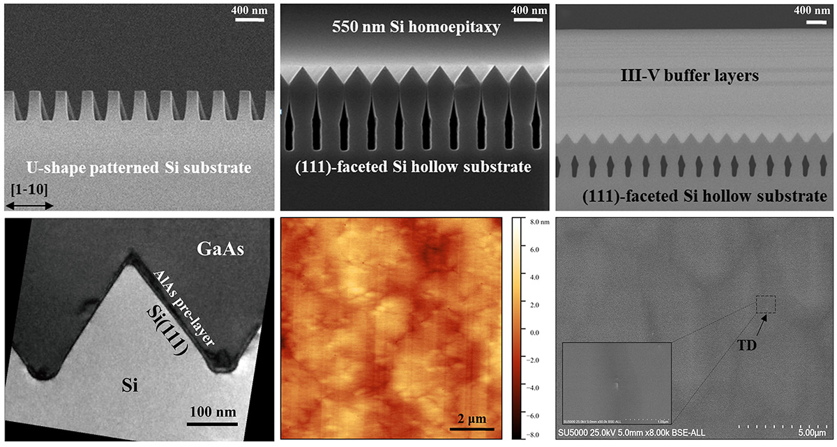
High-quality GaAs layers grown on Si (001) substrates. (A), (B), and (C) Cross-sectional SEM images of the “U”-shaped patterned Si (001), (111)-faceted silicon hollow substrate, and the GaAs/Si (001) substrate, respectively. (D), (E), and (F) Cross-sectional TEM image of the GaAs/Si interface, surface AFM and ECCI images of the GaAs/Si (001) sample, indicating a 1.3 nm RMS (root-mean-square) and a 4.8×106 cm−2 threading dislocation density.
Current usage metrics show cumulative count of Article Views (full-text article views including HTML views, PDF and ePub downloads, according to the available data) and Abstracts Views on Vision4Press platform.
Data correspond to usage on the plateform after 2015. The current usage metrics is available 48-96 hours after online publication and is updated daily on week days.
Initial download of the metrics may take a while.