Figure 3

Download original image
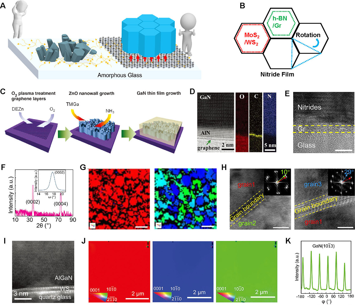
Van der Waals epitaxy. (A) Schematic of graphene lattice-guided nitride film growth on amorphous substrates [63]. (B) Schematic of lattice mismatches between MoS2, WS2, h-BN, and graphene (Gr) with nitrides and grain rotation in the in-plane direction. (C) Diagram of the fabrication process of GaN epitaxial film by introducing Gr layers and ZnO nanowall [4]. (D) HAADF-STEM image of the interface and electron energy loss spectroscopy mappings of O, C, and N elements at the interface [66]. (E) High-resolution transmission electron microscopy (HRTEM) image of the interface of nitrides/Gr/glass [65]. (F) X-ray diffraction (XRD)-2θ scan spectrum of GaN film [65]. (G) Electron backscatter diffraction (EBSD) inverse pole figure (IPF) images of GaN films grown on Gr/glass [65]. (H) HRTEM images of two GaN grains with 10° and 29° relative rotations, respectively [65]. (I) HAADF-STEM image of the interface by introducing WS2 as a buffer layer [67]. (J) EBSD-IPF images of GaN films grown on WS2/glass in the Z-, X-, and Y-directions [67]. (K) XRD-φ scan of GaN from a probed area of 1 mm× 10 mm [67]. The scale bars in (E), (G), (H), and (J) are 5 nm, 1 μm, 5 nm, and 2 μm, respectively.
Current usage metrics show cumulative count of Article Views (full-text article views including HTML views, PDF and ePub downloads, according to the available data) and Abstracts Views on Vision4Press platform.
Data correspond to usage on the plateform after 2015. The current usage metrics is available 48-96 hours after online publication and is updated daily on week days.
Initial download of the metrics may take a while.

